Service

PCB Layout

  • Single-layer, double-layer, multi-layer PCB layout design
  • High-speed digital signal routing
  • Analog circuit design
  • Power electronics layout
  • PCB stacking and interconnect layout
  • EMC/EMI design
  • PCB packaging design
  • Design validation and simulation

PCB Manufacturing

  • Single-layer, double-layer, and multi-layer PCB production
  • High-Density Interconnect (HDI) PCB manufacturing
  • Hard gold plating, soft gold plating, and lead-free processes
  • Solder mask coating and copper plating processes
  • Special materials and thick copper PCB manufacturing
  • Surface Treatment (HASL, ENIG, OSP, Immersion Tin, Immersion Silver etc.)

PCB Assembly

  • Surface Mount Technology (SMT)
  • Through-hole Component Assembly
  • Soldering Techniques (Wave Soldering, Reflow Soldering, etc.)
  • Manual Soldering and Debugging
  • Assembly of BGA and Micro Components
  • Assembly Testing and Functional Testing

PCBA Testing

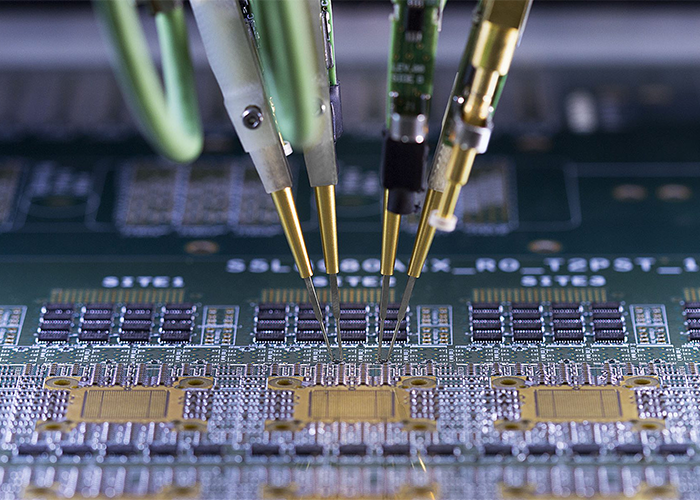
  • Functional Testing: Testing various functions of PCBA products to ensure they meet design requirements.
  • Electrical Testing: Testing the electrical performance of PCBA products, including voltage, current, resistance, etc.
  • Reliability Testing: Conducting long-term stability and reliability testing of PCBA products under different conditions.
  • Environmental Testing: Testing the performance of PCBA products under different environmental conditions such as temperature, humidity, vibration, etc.

Electronic Components

We offer electronic component sourcing services, collaborating with over 500 reliable suppliers to ensure your projects receive the high-quality components they need.

Send Us A Message

  • sandy@jdl-global.com